WITec introduces Ultrafast Confocal Raman Imaging Option
62 500 Raman spectra in less than 2 minutes
Advertisement


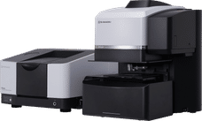
WITec introduces the "ultrafast Raman imaging Option" for the alpha300 R Confocal Raman Microscope. With this option the acquisition time for a single Raman spectrum can be as low as 1.7 milliseconds, according to the company. As a Confocal Raman image typically consists of tens of thousands of spectra, the new option reduces the total acquisition time for a complete image to only a few minutes. For example, a complete hyperspectral image consisting of 250 x 250 pixels = 62,500 Raman spectra can be recorded in less than two minutes. The latest spectroscopic EMCCD detector technology combined with the high throughput optics featured in the alpha300 R Confocal Raman Imaging System are the keys to this improvement. The new option reduces the overall experiment duration and delivers more valuable Raman data in a given time, thereby reducing the total cost of ownership of the system. The improvement in sensitivity can also be advantageous for delicate and precious samples requiring the lowest possible levels of excitation power. Time-resolved investigations of fast dynamic processes can also benefit from the ultrafast spectral acquisition times.
"With this imaging option, WITec sets a new cutting edge standard in acquisition time and sensitivity for confocal Raman Imaging". says Dr. Olaf Hollricher, WITec Managing Director Research and Development. " From now on, hyperspectral Raman Imaging with full spectral information at each image pixel is accessible in only a matter of minutes."
The new Ultrafast Raman Imaging method is available as an optional feature of the alpha300 R confocal Raman Microscope and the confocal Raman imaging upgrades of the alpha300 AFM and SNOM series. In Confocal Raman Imaging, a complete Raman spectrum is acquired at each image pixel. By evaluating dedicated peak characteristics, Raman images can be generated, revealing information on the distribution of the sample's compounds, stress fields or crystallinity. Typical applications for this nondestructive technique can be found in bio-medical and pharmaceutical research, in semiconductors and materials science as well as in nanotechnology.


Other news from the department research and development


These products might interest you