To use all functions of this page, please activate cookies in your browser.
My watch list
my.bionity.com
my.bionity.com
With an accout for my.bionity.com you can always see everything at a glance – and you can configure your own website and individual newsletter.
- My watch list
- My saved searches
- My saved topics
- My newsletter
Laser diode
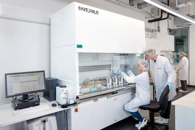
A laser diode is a laser where the active medium is a semiconductor similar to that found in a light-emitting diode. The most common and practical type of laser diode is formed from a p-n junction and powered by injected electrical current. These devices are sometimes referred to as injection laser diodes to distinguish them from optically pumped laser diodes, which are more easily produced in the laboratory. Product highlight
Principle of operationA laser diode, like many other semiconductor devices, is formed by doping a very thin layer on the surface of a crystal wafer. The crystal is doped to produce an n-type region and a p-type region, one above the other, resulting in a p-n junction, or diode. The many, many types of diode lasers known today collectively form a subset of the larger classification of semiconductor p-n junction diodes. Just as in any semiconductor p-n junction diode, forward electrical bias causes the two species of charge carrier, holes and electrons, to be "injected" from opposite sides of the p-n junction into the depletion region, situated at its heart. Holes are injected from the p-doped, and electrons from the n-doped, semiconductor. (A depletion region, devoid of any charge carriers, forms automatically and unavoidably as a result of the difference in chemical potential between n- and p-type semiconductors where ever they are in physical contact.) As charge injection is a distinguishing feature of diode lasers as compared to all other lasers, diode lasers are traditionally and more formally called "injection lasers." (This terminology differentiates diode lasers, e.g., from flashlamp-pumped solid state lasers, such as the ruby laser. Interestingly, whereas the term "solid-state" was extremely apt in differentiating 1950s-era semiconductor electronics from earlier generations of vacuum electronics, it would not have been adequate to convey unambiguously the unique characteristics defining 1960s-era semiconductor lasers.) When an electron and a hole are present in the same region, they may recombine or "annihilate" with the result being spontaneous emission — i.e., the electron may re-occupy the energy state of the hole, emitting a photon with energy equal to the difference between the electron and hole states involved. (In a conventional semiconductor junction diode, the energy released from the recombination of electrons and holes is carried away as phonons, i.e., lattice vibrations, rather than as photons.) Spontaneous emission gives the laser diode below lasing threshold similar properties to an LED. Spontaneous emission is necessary to initiate laser oscillation, but it is one among several sources of inefficiency once the laser is oscillating. The difference between the photon-emitting semiconductor laser or LED (on one hand) and conventional phonon-emitting (non-light-emitting) semiconductor junction diodes (on the other hand) lies in the use of a different type of semiconductor, one whose physical and atomic structure confers the possibility for photon emission. These photon-emitting semiconductors are the so-called "direct bandgap" semiconductors. It is the nature of silicon and germanium, which are single-element semiconductors, that the bandgap does not align in such as way as to be considered "direct." However, the so-called compound semiconductors, which have virtually the identical crystal structure as silicon or germanium but use alternating arrangements of two different atomic species in a checkerboard-like pattern break the symmetry and in doing so create the critical direct bandgap. Examples of compound semiconductors are gallium arsenide, indium phosphide, gallium antimonide, gallium nitride and so forth, and junction diodes fabricated from these materials emit light. In the absence of stimulated emission (e.g., lasing) conditions, electrons and holes may coexist in proximity to one another, without recombining, for a certain time (termed the "upper-state lifetime" or "recombination time," about a nanosecond for typical diode laser materials) before they recombine. Then a nearby photon with energy equal to the recombination energy can cause recombination by stimulated emission. This generates another photon of the same frequency, travelling in the same direction, with the same polarization and phase as the first photon. This means that stimulated emission causes gain in an optical wave (of the correct wavelength) in the injection region, and the gain increases as the number of electrons and holes injected across the junction increases. The spontaneous and stimulated emission processes are vastly more efficient in direct bandgap semiconductors than in indirect bandgap semiconductors, thus silicon is not a common material for laser diodes. As in other lasers, the gain region is surrounded with an optical cavity to form a laser. In the simplest form of laser diode, an optical waveguide is made on that crystal surface, such that the light is confined to a relatively narrow line. The two ends of the crystal are cleaved to form perfectly smooth, parallel edges, forming a Fabry-Perot resonator. Photons emitted into a mode of the waveguide will travel along the waveguide and be reflected several times from each end face before they are emitted. As a light wave passes through the cavity, it is amplified by stimulated emission, but light is also lost due to absorption and by incomplete reflection from the end facets. Finally, if there is more amplification than loss, the diode begins to "lase". Some important properties of laser diodes are determined by the geometry of the optical cavity. Generally, in the vertical direction, the light is contained in a very thin layer, and the structure supports only a single optical mode in the direction perpendicular to the layers. In the lateral direction, if the waveguide is wide compared to the wavelength of light, then the waveguide can support multiple lateral optical modes, and the laser is known as "multi-mode". These laterally multi-mode lasers are adequate in cases where one needs a very large amount of power, but not a small diffraction-limited beam; for example in printing, activating chemicals, or pumping other types of lasers. In applications where a small focused beam is needed, the waveguide must be made narrow, on the order of the optical wavelength. This way, only a single lateral mode is supported and one ends up with a diffraction limited beam. Such single spatial mode devices are used for optical storage, laser pointers, and fiber optics. Note that these lasers may still support multiple longitudinal modes, and thus can lase at multiple wavelengths simultaneously. The wavelength emitted is a function of the band-gap of the semiconductor and the modes of the optical cavity. In general, the maximum gain will occur for photons with energy slightly above the band-gap energy, and the modes nearest the gain peak will lase most strongly. If the diode is driven strongly enough, additional side modes may also lase. Some laser diodes, such as most visible lasers, operate at a single wavelength, but that wavelength is unstable and changes due to fluctuations in current or temperature. Due to diffraction, the beam diverges (expands) rapidly after leaving the chip, typically at 30 degrees vertically by 10 degrees laterally. A lens must be used in order to form a collimated beam like that produced by a laser pointer. If a circular beam is required, cylindrical lenses and other optics are used. For single spatial mode lasers, using symmetrical lenses, the collimated beam ends up being elliptical in shape, due to the difference in the vertical and lateral divergences. This is easily observable with a red laser pointer. The simple diode described above has been heavily modified in recent years to accommodate modern technology, resulting in a variety of types of laser diodes, as described below. Laser diode typesThe simple laser diode structure, described above, is extremely inefficient. Such devices require so much power that they can only achieve pulsed operation without damage. Although historically important and easy to explain, such devices are not practical. Double heterostructure lasers
In these devices, a layer of low bandgap material is sandwiched between two high bandgap layers. One commonly-used pair of materials is gallium arsenide (GaAs) with aluminium gallium arsenide (AlxGa(1-x)As). Each of the junctions between different bandgap materials is called a heterostructure, hence the name "double heterostructure laser" or DH laser. The kind of laser diode described in the first part of the article may be referred to as a homojunction laser, for contrast with these more popular devices. The advantage of a DH laser is that the region where free electrons and holes exist simultaneously—the active region—is confined to the thin middle layer. This means that many more of the electron-hole pairs can contribute to amplification—not so many are left out in the poorly amplifying periphery. In addition, light is reflected from the heterojunction; hence, the light is confined to the region where the amplification takes place. Quantum well lasersIf the middle layer is made thin enough, it acts as a quantum well. This means that the vertical variation of the electron's wavefunction, and thus a component of its energy, is quantised. The efficiency of a quantum well laser is greater than that of a bulk laser because the density of states function of electrons in the quantum well system has an abrupt edge that concentrates electrons in energy states that contribute to laser action. Lasers containing more than one quantum well layer are known as multiple quantum well lasers. Multiple quantum wells improve the overlap of the gain region with the optical waveguide mode. Further improvements in the laser efficiency have also been demonstrated by reducing the quantum well layer to a quantum wire or to a "sea" of quantum dots. In a quantum cascade laser, the difference between quantum well energy levels is used for the laser transition instead of the bandgap. This enables laser action at relatively long wavelengths, which can be tuned simply by altering the thickness of the layer. Separate confinement heterostructure lasersThe problem with the simple quantum well diode described above is that the thin layer is simply too small to effectively confine the light. To compensate, another two layers are added on, outside the first three. These layers have a lower refractive index than the centre layers, and hence confine the light effectively. Such a design is called a separate confinement heterostructure (SCH) laser diode. Almost all commercial laser diodes since the 1990s have been SCH quantum well diodes. Distributed feedback lasersDistributed feedback lasers (DFB) are the most common transmitter type in DWDM-systems. To stabilize the lasing wavelength, a diffraction grating is etched close to the p-n junction of the diode. This grating acts like an optical filter, causing a single wavelength to be fed back to the gain region and lase. Since the grating provides the feedback that is required for lasing, reflection from the facets is not required. Thus, at least one facet of a DFB is anti-reflection coated. The DFB laser has a stable wavelength that is set during manufacturing by the pitch of the grating, and can only be tuned slightly with temperature. Such lasers are the workhorse of demanding optical communication. VCSELsVertical-cavity surface-emitting lasers (VCSELs) have the optical cavity axis along the direction of current flow rather than perpendicular to the current flow as in conventional laser diodes. The active region length is very short compared with the lateral dimensions so that the radiation emerges from the surface of the cavity rather than from its edge as shown in Fig. 2. The reflectors at the ends of the cavity are dielectric mirrors made from alternating high and low refractive index quarter-wave thick multilayer. There are several advantages to producing VCSELs when compared with the production process of edge-emitting lasers. Edge-emitters cannot be tested until the end of the production process. If the edge-emitter does not work, whether due to bad contacts or poor material growth quality, the production time and the processing materials have been wasted. Additionally, because VCSELs emit the beam perpendicular to the active region of the laser as opposed to parallel as with an edge emitter, tens of thousands of VCSELs can be processed simultaneously on a three inch Gallium Arsenide wafer. Furthermore, even though the VCSEL production process is more labor and material intensive, the yield can be controlled to a more predictable outcome. Such dielectric mirrors provide a high degree of wavelength-selective reflectance at the required free surface wavelength λ if the thicknesses of alternating layers d1 and d2 with refractive indices n1 and n2 are such that n1d1 + n2d2 = ½λ which then leads to the constructive interference of all partially reflected waves at the interfaces. But there is a disadvantage because of the high mirror reflectivities, VCSELs have lower output powers when compared to edge emitting lasers. VECSELsVertical external-cavity surface-emitting lasers, or VECSELs, are similar to VCSELs. In VCSELs, the mirrors are typically grown epitaxially as part of the diode structure, or grown separately and bonded directly to the semiconductor containing the active region. VECSELs are distinguished by a construction in which one of the two mirrors is external to the diode structure. As a result, the cavity includes a free-space region. A typical distance from the diode to the external mirror would be 1 cm. One of the most interesting features of any VECSEL is the thin-ness of the semiconductor gain region in the direction of propagation, less than 100 nm. In contrast, a conventional in-plane semiconductor laser entails light propagation over distances of from 250 µm upward to 2 mm or longer. The significance of the short propagation distance is that it causes the effect of "antiguiding" nonlinearities in the diode laser gain region to be minimized. The result is a large-cross-section single-mode optical beam which is not attainable from in-plane ("edge-emitting") diode lasers. Several workers demonstrated optically pumped VECSELs, and they continue to be developed for many applications including high power sources for use in industrial machining (cutting, punching, etc.) because of their unusually high power and efficiency when pumped by multi-mode diode laser bars. Electrically pumped VECSELs have also been demonstrated. Applications for electrically pumped VECSELs include projection displays, served by frequency doubling of near-IR VECSEL emitters to produce blue and green light. Failure modesLaser diodes have similar reliability and failure issues as light emitting diodes. In addition, they are subject to catastrophic optical damage (COD) when operated at higher power. Many of the advances in reliability of diode lasers in the last 20 years remain proprietary to their developers. The reliability of a laser diode can make or break a product line. Moreover, "reverse engineering" is not always able to uncover the differences between more-reliable and less-reliable diode laser products. At the edge of a diode laser, where light is emitted, a mirror is traditionally formed by cleaving the semiconductor wafer to form a specularly reflecting plane. This approach is facilitated by the weakness of the [110] crystallographic plane in III-V semiconductor crystals (such as GaAs, InP, GaSb, etc.) compared to other planes. A scratch made at the edge of the wafer and a slight bending force causes a nearly atomically perfect mirror-like cleavage plane to form and propagate in a straight line across the wafer. But it so happens that the atomic states at the cleavage plane are altered (compared to their bulk properties within the crystal) by the termination of the perfectly periodic lattice at that plane. Surface states at the cleaved plane, have energy levels within the (otherwise forbidden) bandgap of the semiconductor. Essentially as a result, when light propagates through the cleavage plane and transits to free space from within the semiconductor crystal, a fraction of that light energy is absorbed by the surface states whence it is converted to heat by phonon-electron interactions. This heats the cleaved mirror. In addition, the mirror may heat simply because the edge of the diode laser—which is electrically pumped—is in less-perfect contact with the mount that provides a path for heat removal. The heating of the mirror causes the bandgap of the semiconductor to shrink in the warmer areas. The bandgap shrinkage brings more electronic band-to-band transitions into alignment with the photon energy causing yet more absorption. This is thermal runaway, a form of positive feedback, and the result can be melting of the facet, known as catastrophic optical damage, or COD. In the 1970's, this problem, which is particularly nettlesome for GaAs-based lasers emitting between 1 µm and 0.630 µm wavelengths (less so for InP based lasers used for long-haul telecommunications which emit between 1.3 µm and 2 µm), was identified. Michael Ettenberg, a researcher and later Vice President at RCA Laboratories' David Sarnoff Research Center in Princeton, New Jersey, devised a solution. A thin layer of aluminum oxide was deposited on the facet. If the aluminum oxide thickness is chosen correctly it functions as an anti-reflective coating, reducing reflection at the surface. This alleviated the heating and COD at the facet. Since then, various other refinements have been employed. One approach is to create a so-called non-absorbing mirror (NAM) such that the final 10 µm or so before the light emits from the cleaved facet are rendered non-absorbing at the wavelength of interest. In the very early 1990s, SDL, Inc. began supplying high power diode lasers with good reliability characteristics. CEO Donald Scifres and CTO David Welch presented new reliability performance data at, e.g., SPIE Photonics West conferences of the era. The methods used by SDL to defeat COD were considered to be highly proprietary and have still not been disclosed publicly as of June, 2006. In the mid-1990s, IBM Research (Ruschlikon, Switzerland) announced that it had devised its so-called "E2 process" which conferred extraordinary resistance to COD in GaAs-based lasers. This process, too, has never been disclosed as of June, 2006. Reliability of high-power diode laser pump bars (employed to pump solid state lasers) remains a difficult problem in a variety of applications, in spite of these proprietary advances. Indeed, the physics of diode laser failure is still in the process of being worked out and research on this subject remains active, if proprietary. Extension of the lifetime of laser diodes is critical to their continued adaptation to a wide variety of applications. Applications of laser diodesLaser diodes are numerically the most common type of laser, with 2004 sales of approximately 733 million diode lasers,[1] as compared to 131,000 of other types of lasers.[2] Laser diodes find wide use in telecommunication as easily modulated and easily coupled light sources for fiber optics communication. They are used in various measuring instruments, eg. rangefinders. Another common use is in barcode readers. Visible lasers, typically red but later also green, are common as laser pointers. Both low and high-power diodes are used extensively in the printing industry both as light sources for scanning (input) of images and for very high-speed and high-resolution printing plate (output) manufacturing. Infrared and red laser diodes are common in CD players, CD-ROMs and DVD technology. Violet lasers are used in HD-DVD and Blu-Ray technology. High-power laser diodes are used in industrial applications such as heat treating, cladding, seam welding and for pumping other lasers, such as diode pumped solid state lasers. The use of diode lasers for high-speed, low-cost, combustion spectroscopy is being explored. In general, applications of laser diodes can be categorized in various ways. Most applications of diode lasers can be served by larger solid state lasers or optical parametric oscillators but it is the ability to mass-produce diode lasers at low cost that makes them essential for mass-market applications. Diode lasers have application to virtually every field of endeavor that attracts wide attention today. Since light has many different properties (power, wavelength & spectral quality, beam quality, polarization, etc.) it is interesting to classify applications by these basic properties. Many applications of diode lasers primarily make use of the "directed energy" property of an optical beam. In this category one might include the laser printers, bar-code readers, image scanning, illuminators, designators, optical data recording, combustion ignition, laser surgery, industrial sorting, industrial machining, and directed energy weaponry. Some of these applications are emerging whereas many are familiar to the wider society. Applications which may today or in the future make use of the "coherent" properties of diode-laser-generated light include interferometric distance measurement, holography, coherent communications, and coherent control of chemical reactions. Applications which may make use of "narrow spectral" properties of diode lasers include range-finding, telecommunications, infra-red countermeasures, spectroscopic sensing, generation of radio-frequency or terahertz waves, atomic clock state preparation, quantum key cryptography, frequency doubling and conversion, water purification (in the UV), and photodynamic therapy (where a particular wavelength of light would cause a substance such as porphyrin to become chemically active as an anti-cancer agent only where the tissue is illuminated by light). Applications where the ability to "generate ultra-short pulses of light" by the technique known as "mode-locking" include clock distribution for high-performance integrated circuits, high-peak-power sources for laser-induced breakdown spectroscopy sensing, arbitrary waveform generation for radio-frequency waves, photonic sampling for analog-to-digital conversion, and optical code-division-multiple-access systems for secure communication. HistoryThe first to demonstrate coherent light emission from a semiconductor diode (the first laser diode), is widely acknowledged to have been Robert N. Hall and his team at the General Electric research center in 1962.[3] The first visible wavelength laser diode was demonstrated by Nick Holonyak, Jr., later in 1962[4] Other teams at IBM, MIT Lincoln Laboratory, Texas Instruments, and RCA Laboratories were also involved in and receive credit for historic initial demonstrations of efficient light emission and lasing in semiconductor diodes in 1962 and thereafter. In the early 1960s liquid phase epitaxy (LPE) was invented by Herbert Nelson of RCA Laboratories. By layering the highest quality crystals of varying compositions, it enabled the demonstration of the highest quality heterojunction semiconductor laser materials for many years. LPE was adopted by all the leading laboratories, worldwide and used for many years. It was finally supplanted in the 1970s by molecular beam epitaxy and organometallic chemical vapor deposition. Diode lasers of that era operated with threshold current densities of 1000 Amperes per square centimeter at 77°K temperatures. This is a rather modest current density considering that the contact area of diode lasers is a tiny fraction of a square centimeter. Such performance enabled continuous-lasing to be demonstrated in the earliest days. However, when operated at room temperature, 300°K or thereabouts, the threshold current densities were two orders of magnitude greater, or 100,000 Amperes per square centimeter in the best devices. The dominant challenge for the remainder of the 1960s was to obtain low threshold current density at 300°K and thereby to demonstrate continuous-wave lasing at room temperature from a diode laser. The first diode lasers were homojunction diodes. That is, the bandgaps of the waveguide core layer and that of the surrounding clad layers, were identical. It was recognized that there was an opportunity, particularly afforded by the use of liquid phase epitaxy using aluminum gallium arsenide, to introduce heterojunctions. Heterostructures consist of layers of semiconductor crystal having varying bandgap and refractive index. Heterojunctions (formed from heterostructures) had been recognized by Herbert Kroemer, while working at RCA Laboratories in the mid-1950s, as having unique advantages for several types of electronic and optoelectronic devices including diode lasers. LPE afforded the technology of making heterojunction diode lasers. The first heterojunction diode lasers were single-heterojunction lasers. These lasers utilized aluminum gallium arsenide p-type injectors situated over n-type gallium arsenide layers grown on the substrate by LPE. An admixture of aluminum replaced gallium in the semiconductor crystal and raised the bandgap of the p-type injector over that of the n-type layers beneath. It worked; the 300°K threshold currents went down by 10× to 10,000 amperes per square centimeter. Unfortunately, this was still not in the needed range and these single-heterostructure diode lasers did not function in continuous wave operation at room temperature. The innovation that broke the room temperature challenge was the double heterostructure laser. The trick was to quickly move the wafer in the LPE apparatus between different "melts" of aluminum gallium arsenide (p- and n-type) and a third melt of gallium arsenide. It had to be done rapidly since the gallium arsenide core region needed to be significantly under 1 µm in thickness. This may have been the earliest true example of "nanotechnology." The first laser diode to achieve continuous wave operation was a double heterostructure demonstrated in 1970 essentially simultaneously by Zhores Alferov and collaborators (including Dmitri Z. Garbuzov) of the Soviet Union, and Morton Panish and Izuo Hayashi working in the United States. However, it is widely accepted that Zhores I. Alferov and team reached the milestone first. For their accomplishment and that of their co-workers, Alferov and Kroemer shared the 2000 Nobel Prize in Physics. See also
References
|
|
| This article is licensed under the GNU Free Documentation License. It uses material from the Wikipedia article "Laser_diode". A list of authors is available in Wikipedia. |
Last viewed


